A tiny change at the boundary between two oxide layers may point to a less power-hungry future for artificial intelligence.
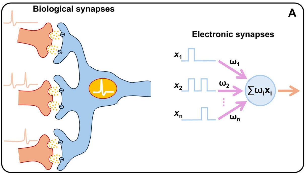
Researchers led by the University of Cambridge have built a nanoelectronic device that behaves a bit like a brain synapse, storing and processing information in the same place instead of shuttling data back and forth as standard computer chips do. That matters because today’s AI hardware burns through vast amounts of electricity, and the demand is still rising.
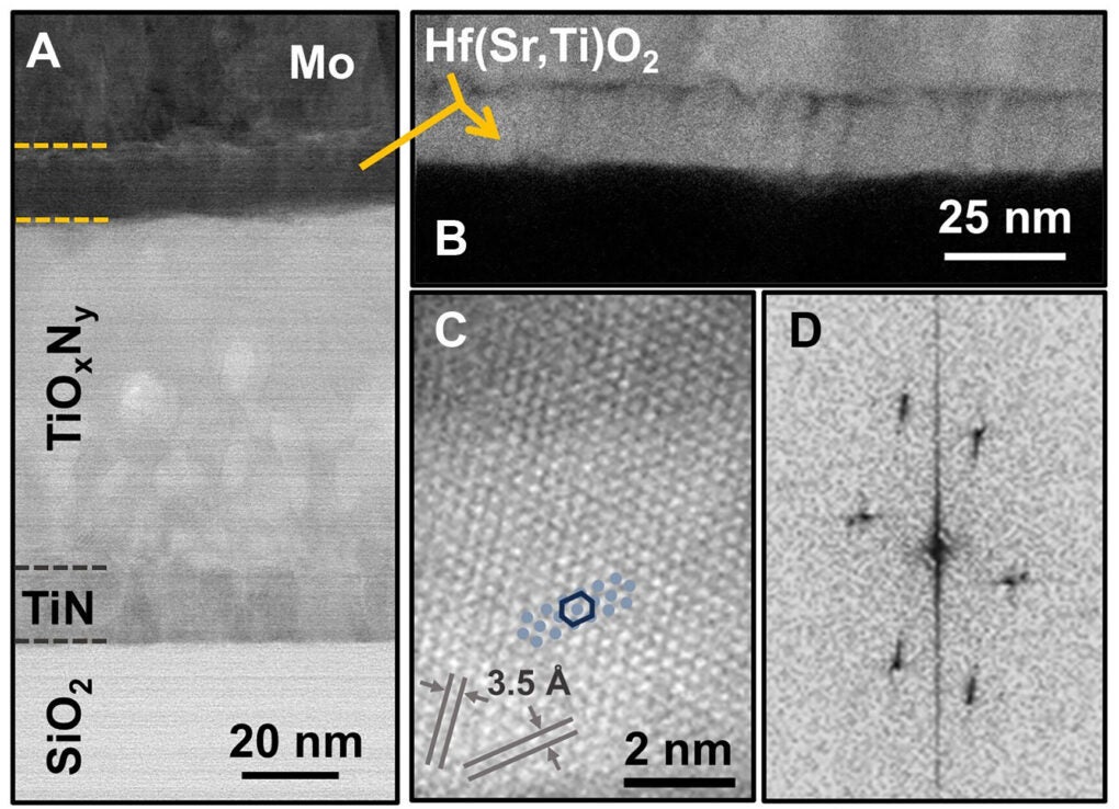
The team’s device is a memristor, a component designed to mimic how neurons and synapses adjust their connections. In this case, the memristor is made from a modified form of hafnium oxide containing strontium and titanium. The work appears in Science Advances.
“Energy consumption is one of the key challenges in current AI hardware,” lead author Dr. Babak Bakhit of Cambridge’s Department of Materials Science and Metallurgy said in a statement. “To address that, you need devices with extremely low currents, excellent stability, outstanding uniformity across switching cycles and devices, and the ability to switch between many distinct states.”
Much of the excitement around neuromorphic computing comes from a simple idea: the brain does not separate memory and computation the way a conventional computer does. In standard chips, that separation forces constant data movement, which costs time and energy. Neuromorphic systems aim to cut that waste, and the source material says compute-in-memory designs could save more than 70% of current computing power consumption.
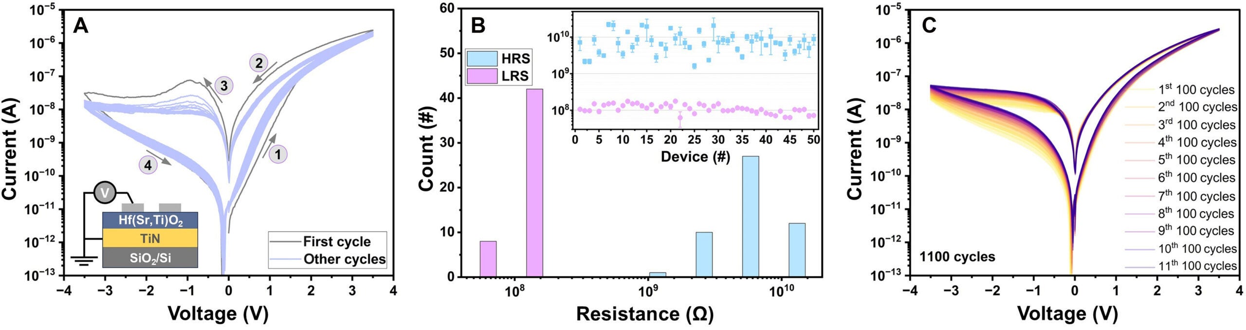
Yet memristors have had a stubborn problem. Many rely on tiny conductive filaments forming inside an oxide. Those filaments can be erratic, varying from one device to the next and even from one cycle to the next. They also often need high voltages to get started and high currents to operate, which is not ideal for energy-efficient AI hardware.
The Cambridge group took a different route. Instead of depending on filament growth and rupture, they built a thin film that switches through what they describe as an interfacial mechanism. Using a two-step growth process, they created a p-n-like junction between p-type Hf(Sr,Ti)O2 and n-type TiOxNy. In plain terms, the key action happens at the interface between layers, where the energy barrier can be tuned smoothly.
“Filamentary devices suffer from random behaviour,” Bakhit said. “But because our devices switch at the interface, they show outstanding uniformity from cycle to cycle and from device to device.”
That smoothness is a big part of the story.
The researchers reported switching currents at or below 10−8 amperes, with measured currents ranging from about 5 × 10⁻⁹ to 9 × 10⁻¹¹ amperes in one estimate of synaptic update energy. They calculated that the energy per update falls in the range of roughly 2.5 picojoules to 45 femtojoules. The devices also produced hundreds of stable, replicable conductance levels, ranging from about 2.5 × 10⁻⁹ to 1.4 × 10⁻⁷ siemens, with a conductance-modulation range above 50.
One sentence in the paper stands out: the devices kept changing conductance over 6,000 applied spikes without saturating.
That gradual tuning matters because neuromorphic hardware works best when it can adjust weights in many small steps, rather than jumping between a few rigid states. In laboratory tests, the memristors also endured more than 10,000 pulse-switching cycles, with one set of data showing stable resistance states up to 5 × 10^4 switching cycles. Binary states remained stable for up to 5 × 10^5 seconds.
The devices also reproduced several learning behaviors associated with biological synapses, including paired-pulse facilitation, paired-pulse depression, short-term synaptic plasticity, and spike-timing dependent plasticity. Those are the kinds of traits engineers want for systems that can learn from timing and sequence, not just store digital bits.
“These are the properties you need if you want hardware that can learn and adapt, rather than just store bits,” Bakhit said.
The paper does not pretend the problem is solved.
One major hurdle is manufacturing temperature. The current process requires about 700 degrees Celsius, which Bakhit said is higher than standard semiconductor manufacturing tolerances. He called that “currently the main challenge” in fabrication, and said the team is working to lower the temperature so the technology can better match industry processes.
There is another limit, too. The study points to promising device-level behavior, but it stops short of a full network-level hardware demonstration. The authors say that remains for future work.
Bakhit said the breakthrough came after years of failed attempts and a late 2024 twist on the deposition method, when oxygen was added only after the first layer had been grown.
“I spent almost three years on this,” he said. “There were a huge number of failures. But at the end of November, we saw the first really good results.”
A patent application has been filed by Cambridge Enterprise. The research was supported in part by the Swedish Research Council, the Royal Academy of Engineering, the Royal Society, and UK Research and Innovation.
If the temperature issue can be solved, this kind of memristor could help make AI hardware that uses far less electricity while handling learning tasks in a more brain-like way.
That could matter for data centers, edge devices, and future AI systems that need to process large amounts of information without driving energy use ever higher.
Research findings are available online in the journal Science Advances.
The original story “New brain-inspired device sharply reduces AI hardware energy use” is published in The Brighter Side of News.
Like these kind of feel good stories? Get The Brighter Side of News’ newsletter.
The post New brain-inspired device sharply reduces AI hardware energy use appeared first on The Brighter Side of News.