The next generation of wireless communication, represented by terahertz technology, promises revolutionary advancements in data transmission.
Operating at terahertz frequencies, these systems offer unprecedented bandwidth, enabling ultra-fast data transfer and communication. However, harnessing this potential requires overcoming significant technical challenges, particularly in managing and utilizing the available spectrum effectively.
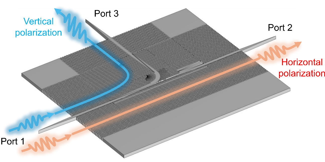
A groundbreaking development addresses this challenge: the first ultra-wideband integrated terahertz polarization (de)multiplexer implemented on a substrateless silicon platform.
This innovation, designed for use in the sub-terahertz J-band (220–330 GHz), is set to transform 6G communications and beyond. The device can effectively double data capacity while maintaining low data loss, paving the way for efficient and reliable high-speed wireless networks.

The team behind this milestone includes Professor Withawat Withayachumnankul from the University of Adelaide’s School of Electrical and Mechanical Engineering, along with Dr. Weijie Gao, now a postdoctoral researcher at Osaka University, and Professor Masayuki Fujita.
“Our proposed polarization multiplexer allows multiple data streams to be transmitted simultaneously over the same frequency band, effectively doubling the data capacity,” said Professor Withayachumnankul. The relative bandwidth achieved by this device is unprecedented in any frequency range, representing a significant leap forward for integrated multiplexers.
Polarization multiplexers are essential in modern communications, as they enable multiple signals to share the same frequency band. This capability significantly increases channel capacity.
The new device achieves this by leveraging tapered directional couplers and anisotropic effective-medium claddings. These components enhance polarization birefringence, leading to a high polarization extinction ratio (PER) and broad bandwidth—essential features for efficient terahertz communication systems.
Related Stories
Unlike traditional designs that rely on complex and frequency-dependent asymmetric waveguides, the new multiplexer uses anisotropic claddings that are only mildly frequency-dependent. This approach fully utilizes the generous bandwidth offered by tapered couplers.
The result is a fractional bandwidth of nearly 40%, with an average PER exceeding 20 dB and minimal insertion loss of about 1 dB. These performance metrics far exceed those of existing optical and microwave designs, which often suffer from narrow bandwidth and higher losses.
The research team’s work not only enhances the efficiency of terahertz systems but also sets the stage for a new era in wireless communications. “This innovation is a key enabler in realizing the full potential of terahertz communications,” noted Dr. Gao. Applications include high-definition video streaming, augmented reality, and next-generation mobile networks like 6G.
Traditional solutions for terahertz polarization management, such as orthomode transducers (OMTs) based on rectangular metallic waveguides, face significant limitations. Metallic waveguides suffer from increased ohmic losses at higher frequencies, and their fabrication is complex due to stringent geometrical requirements.

Optical polarization multiplexers, including those using Mach-Zehnder interferometers or photonic crystals, offer better integrability and lower loss but often involve trade-offs between bandwidth, structural compactness, and fabrication complexity.
Directional couplers, widely used in optical systems, require strong polarization birefringence to achieve compact footprints and high PER. However, they are limited by narrow bandwidth and sensitivity to fabrication tolerances.
The new multiplexer addresses these limitations by combining the advantages of tapered directional couplers and effective-medium claddings. The anisotropic claddings provide substantial birefringence, ensuring high PER across a broad bandwidth. This design principle marks a departure from conventional approaches, offering a scalable and practical solution for terahertz integration.
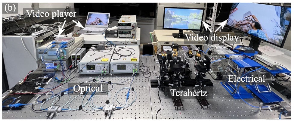
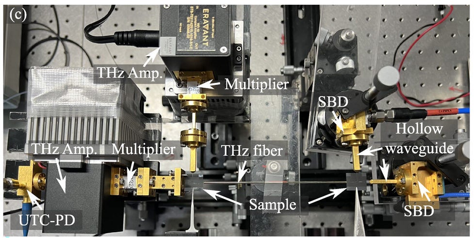
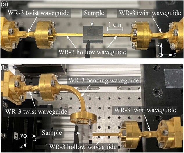
Experimental validation of the multiplexer confirms its remarkable capabilities. The device operates efficiently across 225–330 GHz, achieving a fractional bandwidth of 37.8% and maintaining a PER above 20 dB. Its compact footprint and compatibility with standard fabrication processes make it suitable for large-scale production.

“This innovation not only enhances the efficiency of terahertz communication systems but also paves the way for more robust and reliable high-speed wireless networks,” said Dr. Gao.
The potential applications of this technology extend beyond communication systems. By enabling more efficient spectrum utilization, the multiplexer can drive advancements in fields such as radar, imaging, and the internet of things. “Within a decade, we foresee widespread adoption and integration of these terahertz technologies across various industries,” said Professor Withayachumnankul.
The multiplexer also offers seamless integration with earlier beamforming devices developed by the team, enabling advanced communication functions on a unified platform. This compatibility underscores the versatility and scalability of the effective-medium-clad dielectric waveguide platform.
The team’s work has been published in the journal Laser & Photonic Reviews, highlighting its significance in advancing photonics-enabled terahertz technologies. “By overcoming key technical barriers, this innovation is poised to catalyze a surge of interest and research activity in the field,” said Professor Fujita.

The researchers anticipate that within the next few years, their work will inspire new applications and further technological refinements, ultimately leading to commercial prototypes and products.
This multiplexer represents a major step forward in realizing the full potential of terahertz communications. With its unprecedented performance metrics, it sets a new standard for integrated terahertz devices.
As the demand for high-speed, high-capacity communication networks grows, innovations like this will play a crucial role in shaping the future of wireless technology.
Note: Materials provided above by The Brighter Side of News. Content may be edited for style and length.
Like these kind of feel good stories? Get The Brighter Side of News’ newsletter.
The post Groundbreaking silicon chip unlocks the potential of 6G communications appeared first on The Brighter Side of News.