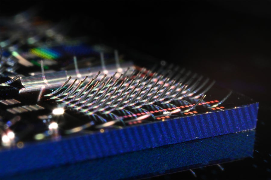
Inside most photonic chips, light races through tiny optical wires. It carries information far faster than electricity can in many conventional systems. But once that light is trapped on the chip, sending it out into open space in a controlled, scalable way becomes much harder. A team led by researchers at MIT and MITRE now says it has built a way around that bottleneck. They did this using microscopic structures that curl upward from the chip surface like ski jumps.
The devices, described in Nature, let researchers steer thousands of tiny laser beams off a chip and into free space with unusual precision. In demonstrations, the team used the platform to project full-color images about half the size of a grain of table salt. Moreover, they used the platform to control diamond-based quantum bits, or qubits, with resonant laser light.
“On a chip, light travels in wires, but in our normal, free-space world, light travels wherever it wants. Interfacing between these two worlds has long been a challenge. But now, with this new platform, we can create thousands of individually controllable laser beams that can interact with the world outside the chip in a single shot,” said Henry Wen, a visiting research scientist in MIT’s Research Laboratory of Electronics, a research scientist at MITRE, and co-lead author of the study.
Wen worked on the paper with co-lead authors Matt Saha of MITRE and Andrew S. Greenspon, a visiting scientist in MIT’s Research Laboratory of Electronics and MITRE. He also worked with Matthew Zimmermann of MITRE, Matt Eichenfield of the University of Arizona, senior author Dirk Englund of MIT, and researchers from Sandia National Laboratories and the University of Arizona.
The work grew out of the Quantum Moonshot Program, a collaboration involving MIT, the University of Colorado Boulder, MITRE, and Sandia National Laboratories. The group has been developing a quantum computing platform based on diamond qubits from Englund’s lab. Those qubits are controlled with laser beams. Furthermore, the long-term challenge is scale.
“We can’t control a million laser beams, but we may need to control a million qubits. So, we needed something that can shoot laser beams into free space and scan them over a large area, kind of like firing a T-shirt gun into the crowd at a sports stadium,” Wen said.
To build that system, the researchers combined silicon nitride and aluminum nitride in a two-layer structure. Because the materials expand and contract differently as they cool after fabrication, the finished structures curl upward. The team also patterned the layers so the bend happens in the direction they want. This creates the “ski-jump” shape that lifts the optical waveguide off the chip and points it outward.
The devices were fabricated on a 200-millimeter wafer in a CMOS foundry. Each cantilever is about 2 micrometers thick and has a submicrogram mass. The study reports mechanical resonances ranging from about 1 kilohertz to more than 100 kilohertz. This helps the structures scan quickly through space.
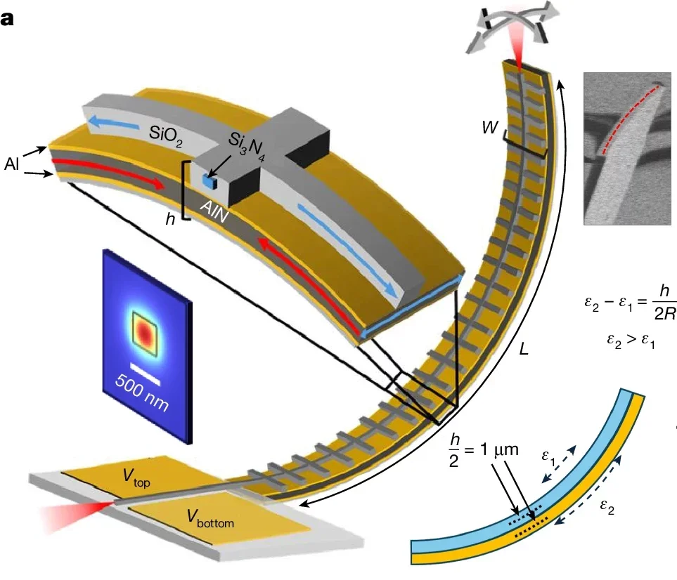
Waveguides on the chip funnel light to the curved structures, and modulators control when that light turns on and off. The team showed broadband transmission from 450 to 750 nanometers and used paired resonances to trace two-dimensional scanning patterns.
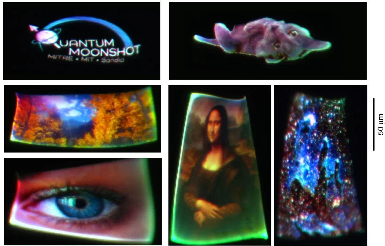
That gave them a way to “paint” in free space. By pulsing off-chip laser diodes, they projected full-color images and video without active stabilization. Wen said the patterns stayed steady enough that the team did not need to correct for drift during operation.
The pixel density is one of the striking claims in the paper. According to Wen, about 30,000 pixels can fit into the area that would hold only two smartphone-display pixels. “Our platform is the ideal optical engine because our pixels are at the physical limit of how small a pixel can be,” he said.
The paper also compares the system with existing beam-scanning technologies. It reports a figure-of-merit improvement of more than 1,000-fold over existing fiber scanners and more than 50-fold over mature MEMS mirrors and acousto-optic deflectors.
One sentence in the paper points to how far the authors think this could go. A compact tiled system with improved performance could support “giga-spot light engines at 1kHz refresh rates in a sub-5-cm diameter chip area.”
The team did more than project images. In one experiment, a ski-jump device directed resonant 737-nanometer light toward diamond waveguides containing negatively charged silicon vacancies. The setup addressed a single emitter with a measured g(2)(0) of 0.09(9), below the 0.5 threshold associated with single-photon emission. The researchers also drove the cantilever at 6.34 kilohertz and reported an extinction ratio of 27.5 decibels.
That matters because fault-tolerant quantum computing would require optical control and readout of huge numbers of qubits. The study argues that is impractical with bulk optics alone.
Still, the technology is not finished. The authors note that current high-performance operation relies on resonant scanning in vacuum, not ordinary ambient conditions. Resonant scanning also lacks true random access. The curved trajectory can create defocusing in optics designed for flat sensors. In addition, practical systems will need solutions for packaging, power handling, and environmental robustness.
Although the team demonstrated stability for more than 15 hours and over one billion cycles in one-dimensional resonant scanning, they say more work is needed on yield, light uniformity, large-array integration, and long-term durability.
If the platform scales as the team hopes, it could make photonic chips much more useful outside their own wiring. That could matter for lightweight augmented reality displays, smaller LiDAR systems for compact robots, faster laser-based 3D printing, and quantum hardware that needs precise optical control over many qubits at once.
The broader significance is simple: a chip that can process light is powerful, but a chip that can also throw that light accurately into the world could be much more versatile.
Research findings are available online in the journal Nature.
The original story “MIT scientists built photonic ‘ski jumps’ that beam light off chips for faster quantum computing” is published in The Brighter Side of News.
Like these kind of feel good stories? Get The Brighter Side of News’ newsletter.
The post MIT scientists built photonic ‘ski jumps’ that beam light off chips for faster quantum computing appeared first on The Brighter Side of News.


Leave a comment
You must be logged in to post a comment.