Photonic chips sit deep inside the modern internet, routing the light pulses that carry emails, videos and AI requests around the world. They are fast, compact and essential. However, they still stumble at some of the most important jobs. This is especially true when light signals need to be converted, amplified or reshaped.
That weakness matters more now than it did a few years ago.
Generative AI systems push far more data back and forth between processors than a standard search query does. Every extra exchange adds pressure on the hardware that moves information inside and between data centers. In addition, what used to be a modest energy cost could become a much larger one. This will happen as AI systems expand and demand more from the networks underneath them.
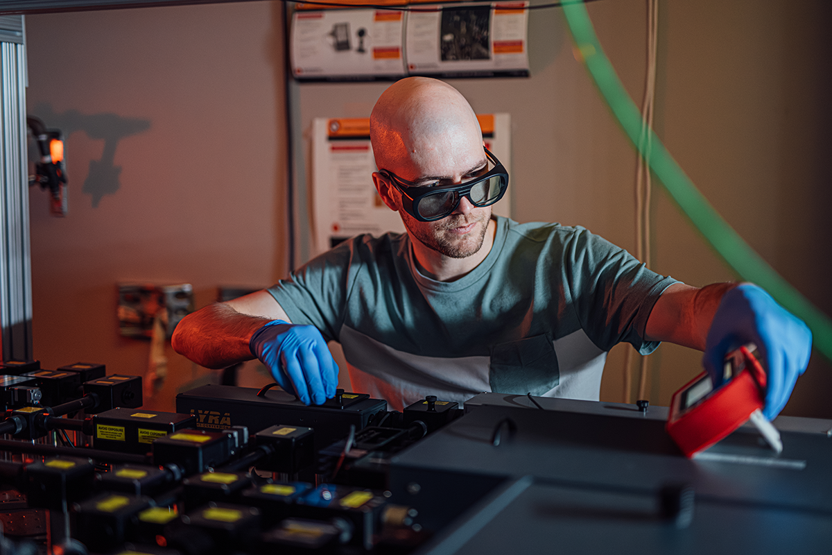
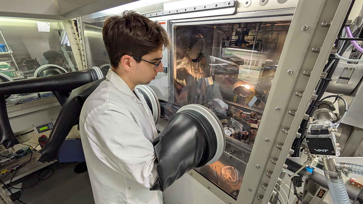
A team at Polytechnique Montréal says it has found a way to give photonic chips some of the functions they have long lacked. Writing in Science Advances, the researchers report a material that can be added directly onto silicon. This material lets light be processed on the chip itself, instead of being repeatedly handed off to extra components.
The work targets a basic limitation in silicon photonics. Silicon is excellent for guiding light, which is why it has become central to optical interconnects, transceivers and other high-bandwidth systems. But it cannot naturally perform certain second-order nonlinear optical functions. These functions are needed for tasks such as light conversion, high-speed modulation and specialized light generation.
To get around that, engineers have generally taken one of two routes. They can build devices from other materials that have those properties, or they can add a second material onto silicon. Both approaches work, but they come with trade-offs in cost, processing temperature, fabrication complexity or compatibility with standard chip manufacturing.
Organic materials have looked attractive because they can be deposited at low temperature on many kinds of surfaces. Yet they have had a problem of their own. To work properly, the molecules in these films usually need to be forced into alignment through electric field poling. This fabrication step adds complexity and requires metal electrodes.
Those electrodes are especially unhelpful in purely optical processes because they take up space and can add optical loss. They do this without doing any useful work.
The Polytechnique Montréal team focused on an organic molecule called triphenylamine-dicyanoquinoxaline, or TPA-QCN. In a thin film made by vacuum evaporation, the molecules spontaneously adopt a preferred orientation instead of remaining randomly arranged. That breaks the symmetry of the film without the need for electric field poling.
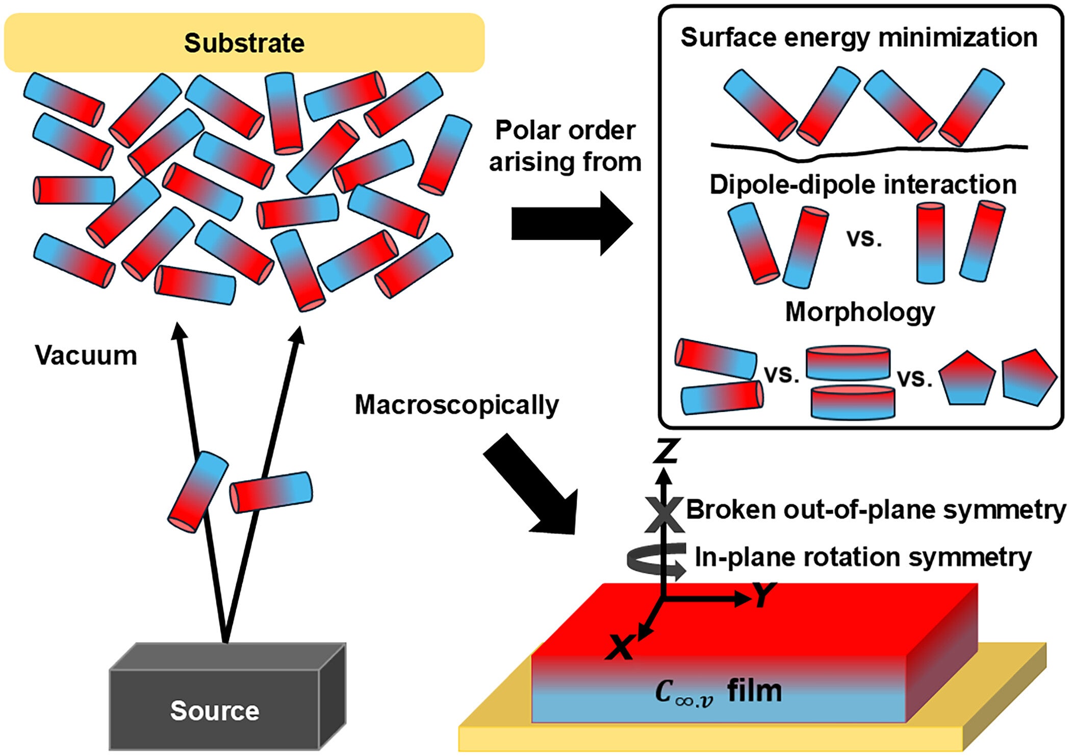
“This spontaneous alignment may sound like a small detail, but physically it makes all the difference,” said engineering physics professor Stéphane Kéna-Cohen. “It gives the material the ability to manipulate light in ways that simply aren’t possible with today’s silicon photonic chips.”
The researchers designed a strip-loaded waveguide using a 230-nanometer TPA-QCN layer on silicon with a thermal oxide buffer. They then showed that the device could convert infrared telecom light at about 1550 nanometers into visible red light near 780 nanometers. Moreover, this conversion happened directly on the chip.
That process, called second-harmonic generation, is a useful test because it depends on the kind of optical nonlinearity the team wanted to unlock.
The material also has a large negative uniaxial birefringence, about minus 0.2, which helped the researchers achieve phase matching between the incoming and converted light. In plain terms, that meant they could keep the two light waves aligned well enough inside the device. As a result, the conversion could happen efficiently.
Simulations suggested the geometry should work with a strip width of 1.9 micrometers, and experiments backed that up. When the team measured the output, the second-harmonic signal followed the expected quadratic relationship with input power. This is a standard sign that the effect came from a second-order nonlinear process.
The phase-matching behavior also shifted in a controlled way as the strip width changed. This was another sign that the device was behaving as designed.

For the best-performing 1.7-millimeter waveguide, the team measured a length-normalized conversion efficiency of 29% W−1 cm−2. The paper says that compares favorably with state-of-the-art strip-loaded thin-film lithium niobate demonstrations. However, it still does not match mature periodically poled monolithic lithium niobate devices.
The result matters not only because the device works, but because it works without electric field poling or periodic patterning. That simplicity is one of the strongest arguments for the approach.
“We can now realistically envision integrating new functions directly onto photonic chips,” said lead author Pierre-Luc Thériault. “And we can do it at low temperature and low cost, using processes that are already standard in the industry.”
The study also points to clear ways to improve performance. The main losses did not appear to come from the material’s intrinsic absorption. Instead, the paper says avoidable leakage into the silicon substrate and lateral leakage of the second-harmonic mode were major contributors. The authors estimate that reducing those losses could raise efficiency by a factor of 2.3, to 68% W−1 cm−2.
Material improvements could push it further. The team notes that related TPA-QCN derivatives have already shown a twofold increase in second-order susceptibility. As a result, this could translate into another fourfold gain in efficiency.
Thermal stability, another practical concern for organic films, also looks promising in the reported tests. TPA-QCN has a glass transition temperature of 110 degrees Celsius, above typical telecom operating temperatures. With a capping layer of TCTA, the film stack kept 90% of its second-harmonic signal up to 129 degrees Celsius. The paper also reports no degradation over 200 days in ambient conditions without encapsulation.
Kéna-Cohen said the larger goal is not to replace electronics, but to reduce the number of extra conversion steps that waste energy and add heat. “If we can combine these functions on a single chip, we simplify everything,” he said. “Fewer conversion steps, less heat, and systems that are better suited for what’s coming.”
That “what’s coming” is the rapid growth of AI hardware that shuttles huge amounts of data between processors. As those exchanges multiply, the cost of moving information becomes harder to ignore.
Photonic chips already carry that burden as the traffic cops of the optical world. What they have lacked is a better way to do more of the job themselves.
This study does not solve that problem overnight. It is a proof of principle, and the reported device still trails the most mature inorganic platforms in raw efficiency. However, it closes a long-standing gap between an intriguing class of organic materials and a working component built in a form that fits modern chipmaking.
The immediate significance is that more optical functions could eventually be built directly onto photonic chips without adding bulky, energy-hungry hardware around them. That could help future data centers move information with less heat and fewer conversion steps. This will be especially relevant as AI systems increase traffic between processors.
Because the material can be deposited at low temperature and is compatible with back-end CMOS processing, the approach may also be easier to fold into existing manufacturing lines. This makes it more accessible than some competing photonic platforms.
Beyond telecom and data infrastructure, the same strategy could support compact modulators, amplifiers, on-chip light sources and components for quantum technologies.
Research findings are available online in the journal Science Advances.
The original story “New material tackles one of the biggest barriers to scaling artificial intelligence” is published in The Brighter Side of News.
Like these kind of feel good stories? Get The Brighter Side of News’ newsletter.
The post New material tackles one of the biggest barriers to scaling artificial intelligence appeared first on The Brighter Side of News.