A display that quietly gathers energy from room light sounds a bit like science fiction, but the underlying physics has pointed in that direction for years.
The basic idea is not hard to grasp. A good semiconductor can emit light efficiently, as in an LED, and absorb light efficiently, as in a solar cell. In principle, one material should be able to do both. In practice, though, engineers have kept running into the same roadblock: the kind of structure that makes one function work well usually weakens the other.
A new study in Joule reports a way around that problem. In work led by Michael McGehee at the University of Colorado Boulder and Jixian Xu at the University of Science and Technology of China, researchers built a reciprocal perovskite diode that performs at a high level in both roles. Used as a solar cell, it reached a certified stabilized power-conversion efficiency of 26.7%. Used as a light-emitting diode, it achieved about 31% external quantum efficiency.
Those numbers would stand out even if the device had been built for only one job.
Metal-halide perovskites have drawn intense attention over the past decade because they can be made relatively cheaply, tuned to different wavelengths of light, and pushed to performance levels that compete with far more expensive semiconductor systems. Yet solar cells and LEDs made from perovskites have mostly developed along separate tracks, even though they use the same material family.
That split came from a stubborn physical mismatch.
An efficient perovskite LED wants an extremely thin and somewhat discontinuous active layer, around 50 nanometers thick. That kind of film helps light escape from the device. A strong solar cell wants something very different, a layer roughly sixteen times thicker, so it can absorb enough incoming sunlight to turn it into electricity.
For years, that thickness gap forced researchers into a choice. If they optimized the device for light emission, it became a weak solar harvester. If they built it to absorb sunlight well, it lost its edge as an LED. Attempts to combine the two usually landed in an awkward middle ground, where neither mode worked especially well.
There was another problem inside the device itself. Even when a perovskite LED generates light successfully, much of that light never escapes. Photons produced inside the material can hit the surface at the wrong angle and get reflected back inward. Once trapped, they bounce around until tiny defects in the material absorb them and convert their energy into heat.
That means a working dual-use device has to solve two issues at once. It has to guide light more effectively, and it has to reduce the defects that waste that light before it can get out.
The team treated those two jobs as parts of the same design problem rather than separate ones.
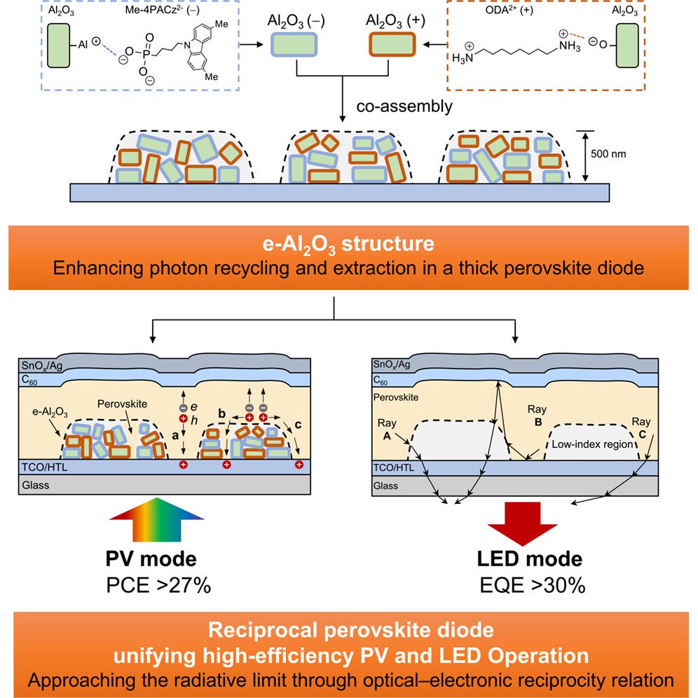
The new architecture builds on earlier work by McGehee and Xu, published in Science in 2023, which showed that porous alumina nanoplates could cut energy losses at perovskite interfaces. This time, the researchers extended that concept into a more elaborate internal structure.
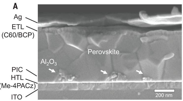
They created micrometer-sized islands of alumina inside the perovskite device. Each island was about five micrometers across and roughly half a micrometer tall. These were not solid lumps. They were porous, more like tiny sponges embedded in the device.
To make them, the team used electrostatic attraction. They prepared two groups of alumina nanoparticles with opposite surface charges. One group was treated with a negatively charged molecule called Me-4PACz. The other was treated with a positively charged molecule called ODA. When mixed, the particles naturally clustered into porous islands. The researchers called the resulting structures e-Al₂O₃, with the “e” standing for electrostatic assembly.
The shape of those islands mattered. Earlier efforts to place low-refractive-index materials into LEDs often interfered with the movement of electrical charge, which hurt performance. Here, the porous structure allowed the perovskite to grow through the alumina islands and maintain electrical contact with the electrode below. The islands could redirect light without cutting off the electrical pathways the device needed.
That alone would have been useful. But the surface chemistry did something else as well.
The same molecules used to give the alumina particles their opposite charges also helped passivate the perovskite surface. In plain terms, they helped neutralize the microscopic defects where energy would otherwise disappear as heat.
That change was dramatic. The surface recombination velocity, which measures how quickly charges are lost at interfaces, fell from 20.2 centimeters per second in a flat control device to 1.4 centimeters per second in the e-Al₂O₃ device. According to the research, that places the interface loss rate close to what is seen in high-performance silicon solar cells.
Once those defects were brought down, another process began to matter more: photon recycling.
This is one of those ideas that sounds technical but follows simple logic. If a photon gets trapped inside the device instead of escaping, that is not necessarily the end of the story. If the material is clean enough, the photon can be reabsorbed and then re-emitted, giving it another chance to find a route out. In a defect-rich material, that would just create more chances to lose energy as heat. In a cleaner one, it becomes an advantage.
The authors report that suppressing recombination this strongly pushed the internal radiative efficiency above 50%. That, in turn, allowed photon recycling to raise external radiative efficiency by more than 40%. The alumina islands also doubled the fraction of photons entering the escape cone, the range of angles that lets light leave the device rather than reflect back inside.
So the structure did more than route light. It made the material good enough for that rerouted light to matter.
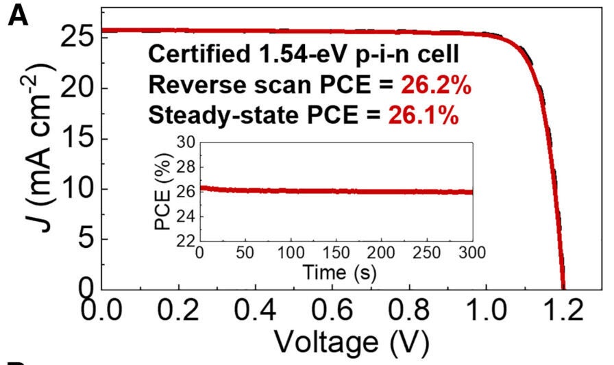
When the researchers operated the device as a solar cell, it delivered a certified stabilized power-conversion efficiency of 26.7%. At the time the work was submitted, that represented the world record for perovskite-device power conversion efficiency, a mark the study says stood from May 2024 to February 2025.
When they ran the same device as an LED, using the same roughly 800-nanometer-thick perovskite layer, it reached an external quantum efficiency of about 31%. In practical terms, that means about 31 out of every 100 injected electrons produced a photon that actually escaped the device. Radiance rose to more than 1,200 watts per steradian per square meter, nearly ten times the level seen in planar control devices.
The researchers also report about 32% LED energy-conversion efficiency, helped by low driving voltage.
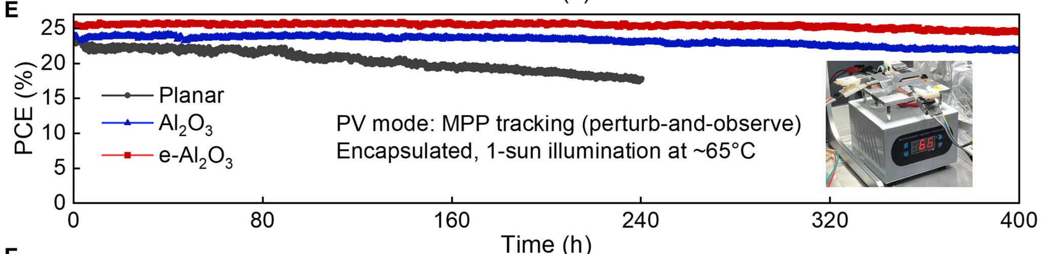
Durability improved as well. In solar-cell mode, the e-Al₂O₃ devices retained 95% of their initial efficiency after 1,200 hours of continuous operation. Flat control devices kept only 67% over the same period. The study also describes the buried interface as stable under both intensive photovoltaic operation and harsh LED operation.
The broader comparison may be the most striking one. According to the authors, this is only the second time that a single polycrystalline device has exceeded 26% efficiency as a solar cell and 30% efficiency as an LED across all photovoltaic materials. The first was single-crystal gallium arsenide, which is much more expensive and far harder to manufacture at scale.
That matters because gallium arsenide is a specialist material. Perovskites are being pursued precisely because they promise something cheaper and more adaptable.
One device, two very different tasks, and little sign of compromise.
The practical appeal is easy to see. A display that harvests ambient light when it is not actively being viewed could offset part of its own energy use. Lighting systems might one day recover energy when they are not serving as light sources. Multifunctional optoelectronic devices start to look more plausible when one architecture can handle both emission and energy harvesting efficiently.
The work also pushes against a deeper assumption in the field. Perovskite LEDs and perovskite solar cells have often been treated as cousins with incompatible needs, linked by chemistry but separated by design. This research argues that the division is not built into the physics. It is a design problem, one that can be tackled by tuning optical behavior and electronic behavior together.
That shift in thinking may matter as much as the record numbers.
Instead of asking whether one device can sacrifice enough to do both jobs, the study asks a different question: what if the same structural features improve both at once?
Here, porous alumina islands helped trapped light escape, lowered interface losses, supported photon recycling, and still preserved the thick absorber needed for solar conversion. The design did not merely split the difference between two technologies. It appears to have used their shared material strengths more effectively than either standard architecture alone.
This work points toward electronic devices that waste less energy by design. The clearest example is a display that could act as a light harvester when idle, trimming battery demand instead of drawing power all the time. The same concept could apply to other optoelectronic systems where light emission and light absorption happen at different moments.
Just as important, the findings offer a route for engineers trying to build devices closer to the radiative limit, where fewer photons are lost as heat and more are used productively. By combining light management and defect passivation in one structure, the research suggests that future perovskite devices may not need to choose so sharply between brightness and power generation.
That makes the result more than a one-off performance milestone. It opens a path toward multifunctional devices that treat light not as a one-way output, but as part of a reversible system.
Research findings are available online in the journal Cell: Joule.
The original story “Perovskite breakthrough brings self-charging screens closer to reality” is published in The Brighter Side of News.
Like these kind of feel good stories? Get The Brighter Side of News’ newsletter.
The post Perovskite breakthrough brings self-charging screens closer to reality appeared first on The Brighter Side of News.